Latest Articles
Auto Switch On for TV
OBJECTIVE
Believe it or not, there are numerous occasions when you have switched. on your TV set to watch a specific program of your interest and you found out that there are still a few more minutes to go. The options before you are to either remain glued on to the TV get and wait for your program or switch off the TV set and then switch it on again after sometime. The first option is boring and with the second, you always run the risk of missing a part of the program if you get busy in something else and forget to switch it on in time. Here is a very simple and interesting gadget that could be very easily mounted on your electrical switchboard and which can be used to perform the auto switch on function for your TV set (or fortran matter any other mains operated system) at a time programmed by you. With this gadget, you could set a timing of 99 minutes maximum with a resolution of one minute. For instance, if you want that your TV set should automatically switch on fifteen minutes from now, all you have got to do is to set l5 in the BCD switches, reset the gadget and press start. Remember that you have to keep the ON/OFF switch on your TV set in the On-position. The gadget can also be bypassed lf you so desired with the help of a switch provided on the gadget itself.

CIRCUIT DESCRIPTION
The circuit shown in Fig. 13.1 is identical to the one described in case of Electronic Reminder gadgetry the previous project except for addition of a power supply section that generates +l2V DC for circuit operation and the output of lC-2B driving an SCR to energise a relay rather than a microbuzzer and an LED as in case of reminder gadget. The ICs used are the same. IC-1 is a Quad 2-input NAND wired as two independent denouncing circuits, 1C-2 is a dual D-type flip flop, IC-3 is a 555 timer generating clock pulses at a rate of one clock pulse per minute, IC-5 and IC6 are programmable Binary/Decade UP/DOWN counters, IC-4 is a Quad 2-input AND gate. All these ICs along with their pin designations and functions have already been discussed at length in project-l2 and shall not be repeated here. The auto switch on gadget operates as follows: Initially, both MASTER RESET (MR) and START outputs are LOW. Set the time in minutes from the BCD switches S4 and S5 after which you want your gadget (TV, VCR etc.) to switch on.
Having programmed the time delay, press and release (Sl) to apply the reset pulse. The positive going reset pulse resets flip flop IC (IC-2) and also loads the programmed time delay information into counter ICs, IC-5 and IC-6. Since the output of IC-2A is initially LOW, the AND-gate is disabled and the clock pulses are not allowed to reach the clock input terminal of counter lC-5 when we press and release (S2), IC-2A is clocked and its output goes HIGH, the AND-gate is enabled and the clock pulses are allowed to the clock input of IC-5, This is the time when the time delay begins. Also, as the power to the TV set or VCR is through the normally open relay contact, the system remains off. We shall not go into the detailed operation of counter ICs but it would suffice to say that (TC) output of IC-6 is normally HIGH and that it would go to LOW state and then HIGH again when the preset time delay has elapsed. This pulse appearing at (TC) output of IC-6 clocks IC2B whose output goes from LOW to HIGH. This LOW to HIGH transition triggers the SCR thus energising relay coil RL-1. The normally open relay contact closes and the system is switched on. The output of IC-2B also forces the Clock Enable (CE) input of IC-5 to go HIGH and disable the clock. The system remains on unless you reset the system.The counters have been wired in the DOWN count mode as it is only then that the counter IC in LSB position completes its count cycle in a number of clock pulses equal to the number set in the LSB BCD switch. The counter connected in MSB position then completes its count cycle in a number of clock pulses equal to ten times the number set in the MSB BCD switch. This gives a total time delay equal to the time period of (N) clock pulses where (N) here is the decimal number preset with the help of BCD switches (S4) and (S5). As the clock period is one minute, the time here can be set in steps of one minute. In essence, maximum time delay that is achievable from the gadget is 99 clock cycles’ Period with a time resolution equal to period of one clock cycle.The power supply section is a conventional step- down transformer, two-diode fpll wave rectifier (using a transformer With a center tapped secondary winding) and a capacitor filter configuration followed by a 12V output three terminal regulator.
CONSTRUCTION GUIDELINES
Figs. 13.2 and 13.3 respectively show the PCB layout and the components layout.


PARTS LIST
Resistors and Capacitors
R1, R2, R3, R4 : 22K 1/4 Watt
R5 : 2.2M 1/4 Watt (Metal film)
R6 : 680K, 1/4 Watt (Metal film)
R7 : 5.6M, 1/4 Watt (Metal film)
R8 : 220K 1/4 Watt (Metal film)
R9 : 1.5K, 1/4 Watt
R10 : 220K, 1/4 Watt
P1 : 100K multitude trimmer potentiometer
C1 : (Ceramic Disc)
C2 : 16V tantalum)
C3: (Ceramic Disc)
C4: Rev (electrolytic)
C5,C7: (Ceramic Disc)
C6 : 16V (Electrolytic)
Semiconductor Device: and ICs
D1 to D4 : 1N4001 or equivalent
IC-1 : CD4011B
IC-2 : CD4013B
lC-3 : 555
IC-4 : CD4081B
IC-5, IC-6 : CD4029B
SCR-1 : OE101 or equivalent
VR-1 : Three terminal Regulator, type 7812
OTHER COMPONENTS
S1 , S2 : Miniature push button microswitches
S3 : Mains power ON/OFF switch
S4, S5 : BCD switches (Thumb- wheel switches)
S6 : ON/OFF switch (230VAC, 1A)
RL-1 : 12DC Relay with at least one normally open contact
T-1 : Mains transformer (Primary: 230VAC Secondary: 14-0-14 250mA)
F-1 : Fuse (0.5A) with holder
Miscellaneous
IC Bases (8 pin, 14pin, 16pin), Multistrand wires, Solder metal, Suitable mounting cabinet, etc.
CLOCK PERIOD ADJUSTMENT, PINCONNECTION DIAGRAMS
Clock period should be precisely adjusted to one minute. The adjustment guidelines are the same as explained in case of Project: 12. The pin connection diagrams of different ICs being used have already beeh given in Project: 12. Pin connections for the SCR are shown in Fin. 13.4.

Believe it or not, there are numerous occasions when you have switched. on your TV set to watch a specific program of your interest and you found out that there are still a few more minutes to go. The options before you are to either remain glued on to the TV get and wait for your program or switch off the TV set and then switch it on again after sometime. The first option is boring and with the second, you always run the risk of missing a part of the program if you get busy in something else and forget to switch it on in time. Here is a very simple and interesting gadget that could be very easily mounted on your electrical switchboard and which can be used to perform the auto switch on function for your TV set (or fortran matter any other mains operated system) at a time programmed by you. With this gadget, you could set a timing of 99 minutes maximum with a resolution of one minute. For instance, if you want that your TV set should automatically switch on fifteen minutes from now, all you have got to do is to set l5 in the BCD switches, reset the gadget and press start. Remember that you have to keep the ON/OFF switch on your TV set in the On-position. The gadget can also be bypassed lf you so desired with the help of a switch provided on the gadget itself.
CIRCUIT DESCRIPTION
The circuit shown in Fig. 13.1 is identical to the one described in case of Electronic Reminder gadgetry the previous project except for addition of a power supply section that generates +l2V DC for circuit operation and the output of lC-2B driving an SCR to energise a relay rather than a microbuzzer and an LED as in case of reminder gadget. The ICs used are the same. IC-1 is a Quad 2-input NAND wired as two independent denouncing circuits, 1C-2 is a dual D-type flip flop, IC-3 is a 555 timer generating clock pulses at a rate of one clock pulse per minute, IC-5 and IC6 are programmable Binary/Decade UP/DOWN counters, IC-4 is a Quad 2-input AND gate. All these ICs along with their pin designations and functions have already been discussed at length in project-l2 and shall not be repeated here. The auto switch on gadget operates as follows: Initially, both MASTER RESET (MR) and START outputs are LOW. Set the time in minutes from the BCD switches S4 and S5 after which you want your gadget (TV, VCR etc.) to switch on.
Having programmed the time delay, press and release (Sl) to apply the reset pulse. The positive going reset pulse resets flip flop IC (IC-2) and also loads the programmed time delay information into counter ICs, IC-5 and IC-6. Since the output of IC-2A is initially LOW, the AND-gate is disabled and the clock pulses are not allowed to reach the clock input terminal of counter lC-5 when we press and release (S2), IC-2A is clocked and its output goes HIGH, the AND-gate is enabled and the clock pulses are allowed to the clock input of IC-5, This is the time when the time delay begins. Also, as the power to the TV set or VCR is through the normally open relay contact, the system remains off. We shall not go into the detailed operation of counter ICs but it would suffice to say that (TC) output of IC-6 is normally HIGH and that it would go to LOW state and then HIGH again when the preset time delay has elapsed. This pulse appearing at (TC) output of IC-6 clocks IC2B whose output goes from LOW to HIGH. This LOW to HIGH transition triggers the SCR thus energising relay coil RL-1. The normally open relay contact closes and the system is switched on. The output of IC-2B also forces the Clock Enable (CE) input of IC-5 to go HIGH and disable the clock. The system remains on unless you reset the system.The counters have been wired in the DOWN count mode as it is only then that the counter IC in LSB position completes its count cycle in a number of clock pulses equal to the number set in the LSB BCD switch. The counter connected in MSB position then completes its count cycle in a number of clock pulses equal to ten times the number set in the MSB BCD switch. This gives a total time delay equal to the time period of (N) clock pulses where (N) here is the decimal number preset with the help of BCD switches (S4) and (S5). As the clock period is one minute, the time here can be set in steps of one minute. In essence, maximum time delay that is achievable from the gadget is 99 clock cycles’ Period with a time resolution equal to period of one clock cycle.The power supply section is a conventional step- down transformer, two-diode fpll wave rectifier (using a transformer With a center tapped secondary winding) and a capacitor filter configuration followed by a 12V output three terminal regulator.
CONSTRUCTION GUIDELINES
Figs. 13.2 and 13.3 respectively show the PCB layout and the components layout.
PARTS LIST
Resistors and Capacitors
R1, R2, R3, R4 : 22K 1/4 Watt
R5 : 2.2M 1/4 Watt (Metal film)
R6 : 680K, 1/4 Watt (Metal film)
R7 : 5.6M, 1/4 Watt (Metal film)
R8 : 220K 1/4 Watt (Metal film)
R9 : 1.5K, 1/4 Watt
R10 : 220K, 1/4 Watt
P1 : 100K multitude trimmer potentiometer
C1 : (Ceramic Disc)
C2 : 16V tantalum)
C3: (Ceramic Disc)
C4: Rev (electrolytic)
C5,C7: (Ceramic Disc)
C6 : 16V (Electrolytic)
Semiconductor Device: and ICs
D1 to D4 : 1N4001 or equivalent
IC-1 : CD4011B
IC-2 : CD4013B
lC-3 : 555
IC-4 : CD4081B
IC-5, IC-6 : CD4029B
SCR-1 : OE101 or equivalent
VR-1 : Three terminal Regulator, type 7812
OTHER COMPONENTS
S1 , S2 : Miniature push button microswitches
S3 : Mains power ON/OFF switch
S4, S5 : BCD switches (Thumb- wheel switches)
S6 : ON/OFF switch (230VAC, 1A)
RL-1 : 12DC Relay with at least one normally open contact
T-1 : Mains transformer (Primary: 230VAC Secondary: 14-0-14 250mA)
F-1 : Fuse (0.5A) with holder
Miscellaneous
IC Bases (8 pin, 14pin, 16pin), Multistrand wires, Solder metal, Suitable mounting cabinet, etc.
CLOCK PERIOD ADJUSTMENT, PINCONNECTION DIAGRAMS
Clock period should be precisely adjusted to one minute. The adjustment guidelines are the same as explained in case of Project: 12. The pin connection diagrams of different ICs being used have already beeh given in Project: 12. Pin connections for the SCR are shown in Fin. 13.4.
Portable Electronic Resistance Meter
OBJECTIVE
A simple, easy to build portable all electronic resistance meter that can be used to accurately measure resistances up to a maximum of 1MΩ is the project under construction here. The circuit operates from twin 9V batteries. The resistance meter has a linear scale and the zero resistance point appears on the extreme left end of the scale. Another significant feature of this meter is that it can be used to measure resistances without actually taking them out of the circuit.It has six different selectable ranges that permit resistance measurement in decades of (i) 1Ω to 10 Ω (ii) 10 Ω t0 100 Ω (iii) 100 Ω to 1K (iv) 1K to 10K (v) 10K to 100K and (vi) 100K to 1M

CIRCUIT DESCRIPTION
The measurement of resistance in this meter is in terms of voltage developed across the unknown resistance due to a constant current flowing through it. The voltage is directly proportional to the unknown resistance value if the current is
constant. Different resistance ranges have been achieved by changing the amplitude of constant current i.e. the current remains constant only for a given resistance range. Also, the constant current amplitude is so chosen that in a given resistance range, it produces a voltage of 0.5Vfor the highest value of resistance in that range. That is, if you have selected a range of say 1K to 10K, then the amplitude of constant current for this range Will be 50 µA. This enables the user to use the meter without taking the components out of the circuit as 0.5V would not operate any of the silicon semiconductor devices (Diodes, Transistors etc.)
The constant current source is constituted by transistor (Q1), diode: (D1) and (D2), Zener diode (VZ1), resistors (R1) to (R7). Resister (R1) provides bias current for the zoner diode (VZ1) and diode (Dl). The amplitude of constant current is given by VZ1 divided by the resistance appearing in the emitter lead of (Q1) as the drop across (D1) cancels the (VBE) drop of (Q1).VZ1is a 5V zener diode and the resistors (R2) to (R7) are so chosen that the amplitudes of constant currents in six different range settings of switch (S1) are 50mA, 5mA, 500 µ A, 50 µ A, 5 µ A and 500nA. Six different ranges are (i) 0 to 10 ohms (ii) 10 ohms to 100 ohms (iii) 100 ohms to 1000 ohms (iv) lKto 10K(v) 10Kto 100K and (vi) 100K to IM. That is, 10Ω, 100Ω, 1000Ω, 10K, 100K and 1M resistors produce 0.5V across them and give full scale deflection in six different range settings. Resistors (R2) to (R7) should be precision resistors (±1% or better) as the accuracy of the instrument largely depends upon precision of these resistors.IC-1 if an opamp and is wired as a non-inverting amplifier with a gain of (1+R9/R8). The gain has been chosen to be (11) to produce 5.5 V at the opamp output for a full scale deflection in the meter. (C1) (C2), C3 and C4 are power supply decoupling capacitors. (P2) is the offset adjust potentiometer for the opamp. This potentiometer is used to calibrate the meter to read zero When a zero (or a short) resistance is connected between the unknown resistance terminals. (P1) is used to calibrate the full scale deflection end of the meter.
CALIBRATION
Connect a small piece of wire between the unknown resistance terminals to simulate a zero resistance. Select any of the resistance ranges.
Potentiometer (P2) is Adjusted to get a zero reading on the meter. Choose 10K full scale deflection range and connect a 10K, ±0.5% or ±1% resistor in place of shorted wire. Adjust (P1) to get full scale deflection on the meter. The meter is calibrated. If you have any difficulty in getting a precision 10K resistor for calibration, you could choose one from a general purpose resistor lot that is within ±0.5% of (OK.
CONSTRUCTION GUIDELINES
Figs. 16.2 and 16.3 respectively show the PCB layout the components layout.


PARTS LIST
Resistors and Capacitors
R1 : 330Ω, 1/4W
R2 : 100 Ω, 1/4W (Metal film)
R3 : 1 K, 1/4W (Metal film)
R4 : 10K, 1/4W (Metal film)
R5 : 100K, 1/4W (Metal film)
R6 : 1M, 1/4W (Metal film)
R7 : 10M, 1/4W (Metal film)
R8 : 1K, 1/4W
R9 : 10K, 1/4W
R10 : 10K , 1/4W
R11 : 1 K, 1/4W
P1, P2 : 10K, Multiturn trimmer potentiometer
C1 , C2 : 0.1µF (Ceramic disc)
C3, C4 : 10µF, 16V (Electrolytic)
Semiconductor Devices and its
D1, D2 : 1N4001 or equivalent
VZ1 : 5V, 400mW zener diode
IC-1 : opamp741 Q1 : 2N2907
Other components
Battery : Two 9V batteries
S1 : Rotary switch with one pole and at least six throws
S2 : DPDT switch
Meter : Meter with 1mA f.s.d.
Miscellaneous
8-pin D.I.L. IC base (1 No.), Multistrand wires, solder metal, leads with crocodile clips, suitable mounting cabinet.
A simple, easy to build portable all electronic resistance meter that can be used to accurately measure resistances up to a maximum of 1MΩ is the project under construction here. The circuit operates from twin 9V batteries. The resistance meter has a linear scale and the zero resistance point appears on the extreme left end of the scale. Another significant feature of this meter is that it can be used to measure resistances without actually taking them out of the circuit.It has six different selectable ranges that permit resistance measurement in decades of (i) 1Ω to 10 Ω (ii) 10 Ω t0 100 Ω (iii) 100 Ω to 1K (iv) 1K to 10K (v) 10K to 100K and (vi) 100K to 1M
CIRCUIT DESCRIPTION
The measurement of resistance in this meter is in terms of voltage developed across the unknown resistance due to a constant current flowing through it. The voltage is directly proportional to the unknown resistance value if the current is
constant. Different resistance ranges have been achieved by changing the amplitude of constant current i.e. the current remains constant only for a given resistance range. Also, the constant current amplitude is so chosen that in a given resistance range, it produces a voltage of 0.5Vfor the highest value of resistance in that range. That is, if you have selected a range of say 1K to 10K, then the amplitude of constant current for this range Will be 50 µA. This enables the user to use the meter without taking the components out of the circuit as 0.5V would not operate any of the silicon semiconductor devices (Diodes, Transistors etc.)
The constant current source is constituted by transistor (Q1), diode: (D1) and (D2), Zener diode (VZ1), resistors (R1) to (R7). Resister (R1) provides bias current for the zoner diode (VZ1) and diode (Dl). The amplitude of constant current is given by VZ1 divided by the resistance appearing in the emitter lead of (Q1) as the drop across (D1) cancels the (VBE) drop of (Q1).VZ1is a 5V zener diode and the resistors (R2) to (R7) are so chosen that the amplitudes of constant currents in six different range settings of switch (S1) are 50mA, 5mA, 500 µ A, 50 µ A, 5 µ A and 500nA. Six different ranges are (i) 0 to 10 ohms (ii) 10 ohms to 100 ohms (iii) 100 ohms to 1000 ohms (iv) lKto 10K(v) 10Kto 100K and (vi) 100K to IM. That is, 10Ω, 100Ω, 1000Ω, 10K, 100K and 1M resistors produce 0.5V across them and give full scale deflection in six different range settings. Resistors (R2) to (R7) should be precision resistors (±1% or better) as the accuracy of the instrument largely depends upon precision of these resistors.IC-1 if an opamp and is wired as a non-inverting amplifier with a gain of (1+R9/R8). The gain has been chosen to be (11) to produce 5.5 V at the opamp output for a full scale deflection in the meter. (C1) (C2), C3 and C4 are power supply decoupling capacitors. (P2) is the offset adjust potentiometer for the opamp. This potentiometer is used to calibrate the meter to read zero When a zero (or a short) resistance is connected between the unknown resistance terminals. (P1) is used to calibrate the full scale deflection end of the meter.
CALIBRATION
Connect a small piece of wire between the unknown resistance terminals to simulate a zero resistance. Select any of the resistance ranges.
Potentiometer (P2) is Adjusted to get a zero reading on the meter. Choose 10K full scale deflection range and connect a 10K, ±0.5% or ±1% resistor in place of shorted wire. Adjust (P1) to get full scale deflection on the meter. The meter is calibrated. If you have any difficulty in getting a precision 10K resistor for calibration, you could choose one from a general purpose resistor lot that is within ±0.5% of (OK.
CONSTRUCTION GUIDELINES
Figs. 16.2 and 16.3 respectively show the PCB layout the components layout.
PARTS LIST
Resistors and Capacitors
R1 : 330Ω, 1/4W
R2 : 100 Ω, 1/4W (Metal film)
R3 : 1 K, 1/4W (Metal film)
R4 : 10K, 1/4W (Metal film)
R5 : 100K, 1/4W (Metal film)
R6 : 1M, 1/4W (Metal film)
R7 : 10M, 1/4W (Metal film)
R8 : 1K, 1/4W
R9 : 10K, 1/4W
R10 : 10K , 1/4W
R11 : 1 K, 1/4W
P1, P2 : 10K, Multiturn trimmer potentiometer
C1 , C2 : 0.1µF (Ceramic disc)
C3, C4 : 10µF, 16V (Electrolytic)
Semiconductor Devices and its
D1, D2 : 1N4001 or equivalent
VZ1 : 5V, 400mW zener diode
IC-1 : opamp741 Q1 : 2N2907
Other components
Battery : Two 9V batteries
S1 : Rotary switch with one pole and at least six throws
S2 : DPDT switch
Meter : Meter with 1mA f.s.d.
Miscellaneous
8-pin D.I.L. IC base (1 No.), Multistrand wires, solder metal, leads with crocodile clips, suitable mounting cabinet.
Digital Stopwatch
OBJECTIVE
The project under construction here is a DIGITAL STOPWATCH that could count time up to a maximum of 99.9 seconds with a resolution of 0.1sec (or in steps of 0.1 sec) or up to a maximum of 999 seconds with a resolution of 1 second.
This has been possible by having two clock frequency options, a 10Hz clock and a 1Hz clock. This gadget can be used to accurately measure short time intervals. It is portable and operates from four rechargeable Ni-Cd cells.

CIRCUIT DESCRIPTION
IC1 (MM5369) is a popular IC used for generating clock pulses in digital time pieces. lC-1 along with resistors (R1), capacitors (C1) and (C2) and crystal generates a 60 Hz clock signal at its output (Pin-1). This 60Hz clock signal is passed on to the clock input of IC-3 (CD4018B) via an arrangement of NAND-gates. It is easy to see that whenever the START switch is pressed momentarily, pin-4 and thus pin-: of IC-2 goes HIGH which enables the NAND-gate designated .IC-2A with the result that the clock signal is
passed onto the IC-3 clock input. When STOP switch (S2) is pressed momentarily, the NAND gate designated IC-2A is disabled due to pin-4 of IC-2 going LOW with the result that the clock pulses are not allowed to reach lC-3. IC-3 and IC4 (CD4018B) are presentable divide by (N) counters where (N) could be 2, 3, 4, 5, 6, 7, 8, 9 or 10. IC-3 here has been wired as a divide byes counter by feeding (Q3) output to Data input of the IC. IC-4 has been wired as a divide-by-10 counter by feeding (Q5) output back to the Data input. With 60Hz clock input to IC-3, we get a 10Hz clock signal at IC-3output which when fed to the lC-4 as the clock signal results in a 1Hz clock signal at the output of IC-4.IC-5, lC-6 and 1C-7 (CD4510B) are presentable UP/DOWN BCD decade counters. These counters are connected in cascade arrangement and can count up to a maximum of 999 clock pulses. When fed with a l Hz clock, the maximum attainable time delay between start and stop operations is thus 999 seconds. Similarly, when the .clock frequency is chosen to be 10Hz, the maximum attainable time delay is 99.9 seconds. The RESET switch can be used to reset the counter to all zeros before start. Usually, the reset terminal is at GND, it is momentarily connected to +5V to reset the counter.IC-8, lC-9 and lC-10 (CD4511B) are BCD to seven segment latch decodes drivers. IC CD4511B can directly drive seven segment LED displays of the common cathode variety.
IC-11, IC-12 and lC-13 (LT543) are seven segment displays of common cathode type. R5 to R25 are current limiting resistors.
CONSTRUCTION GUIDELINES
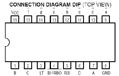
Figs. 17.2 and 17.3 receptively show the PCB layout and the components layout. Pin connection diagrams of CD4510B, CD4511B, CD4011B and LT543 are respectively shown in Figs. 17.4, 17.5,
17.6 and 17.7.


PARTS LIST
Resistors & capacitors
R1 : 22M, 1/4W
R2, R26 : 1K, 1/4W
R3, R4 : 22K 1/4W
R5 to R25 : 680Ω, 1/4W
C1, C2 : 33pF (Ceramic)
C3 : 0.0022µF (Ceramic)
Semiconductor Devices and lCs
D1 : LED
IC-1 : MM5369
lC-2 : CD4011B
IC-3, IC-4 : CD4018B
IC-5, lC-6, IC-7 : CD4510B
IC-8, IC-9, IC-10 : CD4511B
IC-11 , lC-12, IC-13 : LT543 (Common cathode seven segment display) Other comments X-TAL : 3.5795 MHZ crystal
S1, 52 : Miniature push button micro switches
S3, S4 : SPDT switch
S5 : ON/OFF switch
Miscellaneous
IC Bases (14-pin, 16-pin), Nickel-cadmium Cells (4 Nos.), Multistrand wires, solder metal, suitable mounting cabinet.
The project under construction here is a DIGITAL STOPWATCH that could count time up to a maximum of 99.9 seconds with a resolution of 0.1sec (or in steps of 0.1 sec) or up to a maximum of 999 seconds with a resolution of 1 second.
This has been possible by having two clock frequency options, a 10Hz clock and a 1Hz clock. This gadget can be used to accurately measure short time intervals. It is portable and operates from four rechargeable Ni-Cd cells.
CIRCUIT DESCRIPTION
IC1 (MM5369) is a popular IC used for generating clock pulses in digital time pieces. lC-1 along with resistors (R1), capacitors (C1) and (C2) and crystal generates a 60 Hz clock signal at its output (Pin-1). This 60Hz clock signal is passed on to the clock input of IC-3 (CD4018B) via an arrangement of NAND-gates. It is easy to see that whenever the START switch is pressed momentarily, pin-4 and thus pin-: of IC-2 goes HIGH which enables the NAND-gate designated .IC-2A with the result that the clock signal is
passed onto the IC-3 clock input. When STOP switch (S2) is pressed momentarily, the NAND gate designated IC-2A is disabled due to pin-4 of IC-2 going LOW with the result that the clock pulses are not allowed to reach lC-3. IC-3 and IC4 (CD4018B) are presentable divide by (N) counters where (N) could be 2, 3, 4, 5, 6, 7, 8, 9 or 10. IC-3 here has been wired as a divide byes counter by feeding (Q3) output to Data input of the IC. IC-4 has been wired as a divide-by-10 counter by feeding (Q5) output back to the Data input. With 60Hz clock input to IC-3, we get a 10Hz clock signal at IC-3output which when fed to the lC-4 as the clock signal results in a 1Hz clock signal at the output of IC-4.IC-5, lC-6 and 1C-7 (CD4510B) are presentable UP/DOWN BCD decade counters. These counters are connected in cascade arrangement and can count up to a maximum of 999 clock pulses. When fed with a l Hz clock, the maximum attainable time delay between start and stop operations is thus 999 seconds. Similarly, when the .clock frequency is chosen to be 10Hz, the maximum attainable time delay is 99.9 seconds. The RESET switch can be used to reset the counter to all zeros before start. Usually, the reset terminal is at GND, it is momentarily connected to +5V to reset the counter.IC-8, lC-9 and lC-10 (CD4511B) are BCD to seven segment latch decodes drivers. IC CD4511B can directly drive seven segment LED displays of the common cathode variety.
IC-11, IC-12 and lC-13 (LT543) are seven segment displays of common cathode type. R5 to R25 are current limiting resistors.
CONSTRUCTION GUIDELINES
Figs. 17.2 and 17.3 receptively show the PCB layout and the components layout. Pin connection diagrams of CD4510B, CD4511B, CD4011B and LT543 are respectively shown in Figs. 17.4, 17.5,
17.6 and 17.7.
PARTS LIST
Resistors & capacitors
R1 : 22M, 1/4W
R2, R26 : 1K, 1/4W
R3, R4 : 22K 1/4W
R5 to R25 : 680Ω, 1/4W
C1, C2 : 33pF (Ceramic)
C3 : 0.0022µF (Ceramic)
Semiconductor Devices and lCs
D1 : LED
IC-1 : MM5369
lC-2 : CD4011B
IC-3, IC-4 : CD4018B
IC-5, lC-6, IC-7 : CD4510B
IC-8, IC-9, IC-10 : CD4511B
IC-11 , lC-12, IC-13 : LT543 (Common cathode seven segment display) Other comments X-TAL : 3.5795 MHZ crystal
S1, 52 : Miniature push button micro switches
S3, S4 : SPDT switch
S5 : ON/OFF switch
Miscellaneous
IC Bases (14-pin, 16-pin), Nickel-cadmium Cells (4 Nos.), Multistrand wires, solder metal, suitable mounting cabinet.
31 by2 digit Voltmeter with LED Display

OBJECTIVE
The objective here is to build a 3l/2-digit digital voltmeter with a standard instrument sized LED display. It may be mentioned here that the IC type number ICL7107 is almost universally used for digital voltmeter application and the cirduit shown in Fig. 18.1 is basically what you would discover inside any digital panel meter with a 3l/2-digit LED display. The said voltmeter has beep designed to operate from AC mains to generate regulated +5VDC and -5DVC for the circuit.
Digital panel meters with an LED display usually operate from AC mains due to significant current drive requirement of LED displays. There is a separate power supply section (Fig. 18.2) that generates regulated +5VDC and -VDC It is also worthwhile mentioning here that this circuit can also be used for the digital display of any electrical or non-electrical quantity that can be converted into a proportional DC voltage. Digital pH-meters, Pressure meters, Digital Thermometers etc. are all built around the basic circuit shown in Fig. 18.1. The digital voltmeter circuit shown in Fig. 18.1 along with the power supply section of Fig. 18.2 can be used to measure DC voltages over a range of 0 to 1000 VDC It also had a provision of measuring the AC mains voltage RMS value.
CIRCUIT DESCRIPTION
IC lCL7107 from INTERSIL is the heart of the system. Without going into the internal circuit details of this IC, it would suffice to mention here that the said IC is basically a dual slope integrating A/D converter with its own on-chip oscillator (that serves as the clock), reference, decoder and driver and it is capable of driving directly an instrument ‘sized LED display of the common- anode type. The display reading depends upon the analog input voltage and the reference voltage.
The reference voltage is so adjusted that the display reads the analog input directly. In the circuit shown in Fig. 18.1, switch S2 can be used to select DC or AC measurement. When the switch is on AC position, what is actually fed to the analog input terminals of the 1C7107 is the rectified (full wave) AC input after the voltage divider arrangement constituted by resistor (R5) and potentiometer (P2). We shall discuss the adjustment of (P2) under the heading of CALIBRATION. Similarly, when the AC/DC select switch (S2) is on DC, what gels applied to the analog input terminals of the 1C7107 is the DC input divided by the voltage divider arrangement constituted by (R6) and (P3). Adjustment of (P3) will be discussed when we discuss the calibration procedure. The power supply section (Fig. 18.2) is a conventional AC/DC power supply using a step down center tapped mains transformer (T-1), full wave rectifier circuits (D1 and D2 for positive output, D3 and D4 for negative output) and capacitor filters (C1 for positive output and C2 for negative output). Regulation is achieved using three terminal regulators (VR-1) for posltive output and VR-2 for negative output). C3′ to C6 are decoupling capacitors.
CALIBRATION PROCEDURE
The calibration procedure is as follows:
1. Select the AC/DC switch (S2) to be on DC position, feed 100 VDC from a high voltage power supply at DC IN terminals. Adjust potentiometer (P3) to get 2VDC at point-! of the SPDT switch (S2). If 1000VDC is not available, a lower DC voltage can also be used and in that case, the divided voltage should also be proportionately reduced. For instance, for 100 VDC input, the divided voltage will be 200mV. In other words, (P3) should be so adjusted that (R6) and (P3) give a voltage division by a factor of 500.
2. Now, as a second step, adjust potentiometer (P1) so that the meter directly reads the DC input voltage.
3. Change the AC/DC select switch to AC position. Feed AC mains voltage at the AC IN terminals. Adjust potentiometer (P2) so that display directly reads RMS value of the AC input. Before feeding the AC mains, the RMS value of the AC mains should be checked independently with another voltmeter or multimeter with AC voltage measuring capability. – 4. The voltmeter is now calibrated and ready for else.
5. The calibration of this voltmeter should be checked at regular intervals as it may get disturbed due to inherent change in the resistance values of voltage divider resistors.
You may be required to readjust different potentiometers to restore calibration.
CONSTRUCTION GUIDELINES
Figs 18.3 and 18.4 respectively show the PCB layout and the Components layout.

PARTS LIST
Resistors and Capacitors
R1 :470K,1/4W
R2 : IM, 1/4W
R3 :22K 1/4W
R4 :100K, 1/4W
R5 :1M, 15000V (You can also use three 330K 1/2W resistors in series)
R6 :2.2M 1W 1500V resistor
P1 :1 K Preset
P2, P3 :10K Preset
C1, C2 :100µF 16V (Electrolytic)
C3 to C4 :0.1 µF(Ceramic disc)
C7 :0.2 µF (polyester)
C8 :0.47 µF (Polyester)
C9 :0.01 µF(Ceramic disc)
C10 :0.1 µF (Ceramic disc)
C11 :100 µF (Polyester)
Semiconductor Devices and ICS
D1 to D8 : 1N4007 or equivalent
VR-1 :7805 (Three terminal regulator)
VR-2 :7905 (Three terminal regulator)
IC-1 : ICL 7107
Display
(DL-I to DL-4) : Common anode display type no. LTS-542
Other Components
S1 : Mains ON/OFF switch
S2 : SPDT switch, 230V, 1A F1 : Fuse, IA rating with fuse holder
T-1 : Mains transformer (Primary: 230VAC Secondary: 7.5-0-7.5,
500mA)
Miscellaneous
Solder metal, multistrand wires, suitable mounting cabinet.
Pin Connection Diagram of Display
Fig. 18.5 shows the pin connection diagram of seven segment display type no. LTS-542.


Great effort
ReplyDeleteTayyab Siddiqui